¶ KiCad Workflow
The typical workflow in kicad consists in two main tasks: drawing an schematic and then laying out a circuit board from this schematic.
¶ Schematic:

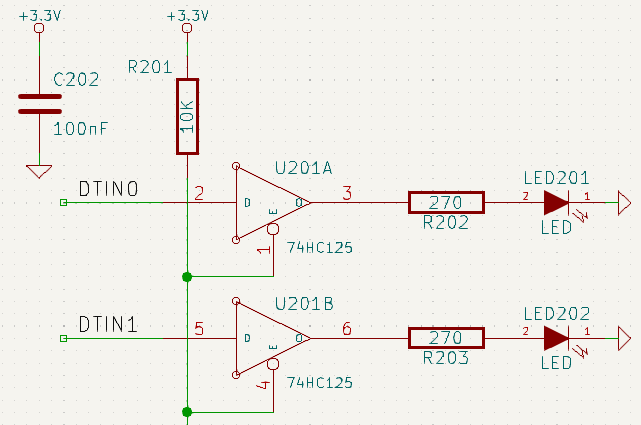
- The schematic is a symbolic representation of the circuit: which components are used and what connections are made between them.
- The schematic contains symbols for every component in the design, with wires connecting pins in the symbols.
- The schematic is typically drawn first, before laying out the circuit board.
¶ Circuit board:

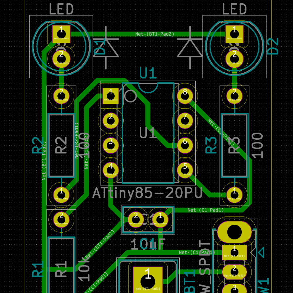
- The circuit board is the physical realization of the schematic, with component footprints positioned on the board and copper tracks making the connections described in the schematic.
- Footprints are a set of copper pads that match the pins on a physical component. When the board is manufactured and assembled, the component will be soldered onto its corresponding footprint on the circuit board.